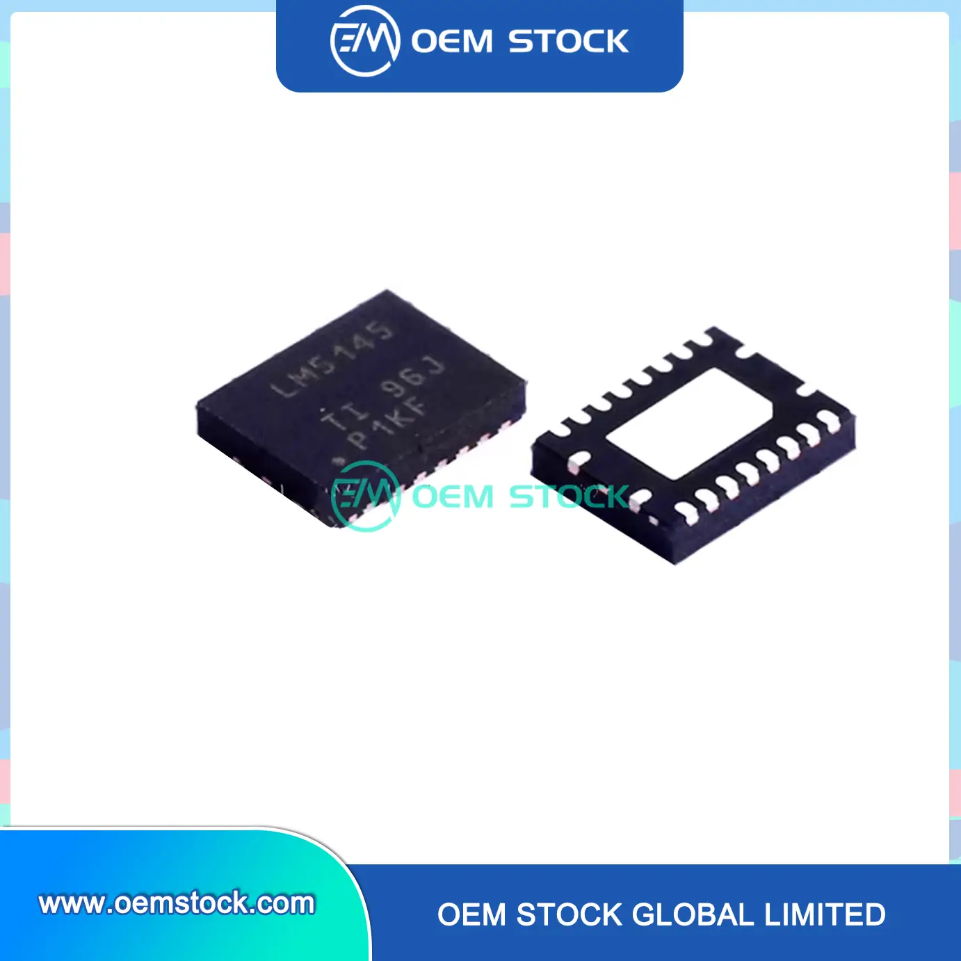

 LM5155DSSR.pdf
Unit Price:$0
Ext Price:$0


The LM5155DSSR belongs to TI's next-generation wide-VIN controller family. It combines peak current-mode control, low IQ and rich protection features in a compact package, enabling robust and space-efficient power stages.
Operates from 3.5 V to 42 V, covering 12 V/24 V automotive rails, industrial buses and battery-powered systems that experience cold-crank and load-dump conditions.
Uses peak current-mode PWM for simpler compensation, inherent current limiting and excellent load-transient performance in boost, SEPIC or flyback converters.
An eco-mode architecture keeps quiescent current very low at light loads, improving efficiency in modules that spend long periods in standby or sleep modes.
Programmable switching frequency up to 2.2 MHz allows designers to shrink magnetics and output capacitors, achieving high power density and small PCB area.
Integrated under-voltage lockout (UVLO), cycle-by-cycle current limit, output over-voltage protection, soft-start and thermal shutdown help protect both the IC and external components in harsh operating environments.
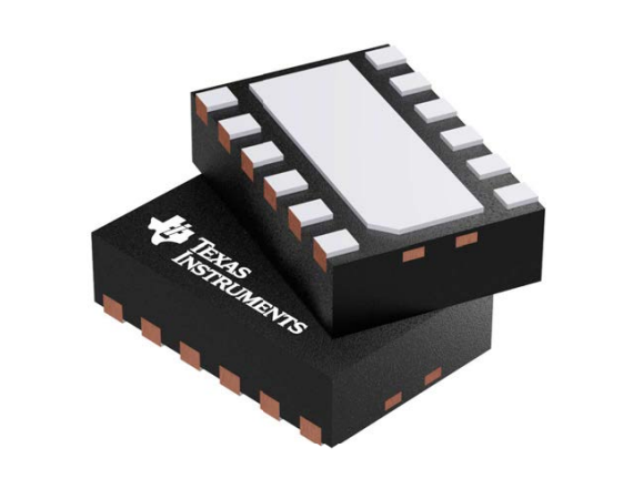
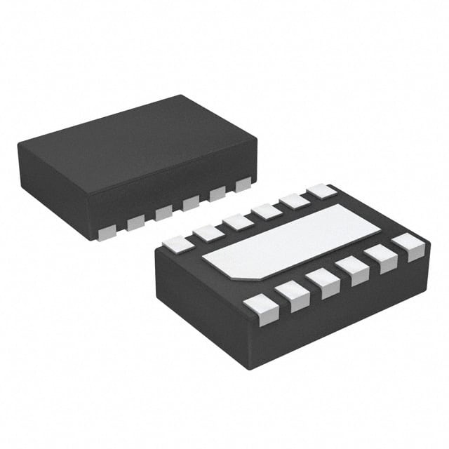
Housed in a thermally enhanced 12-pin WFDFN with exposed pad, the LM5155DSSR offers excellent heat spreading and enables compact layouts in high-current designs.
| Input Voltage Range | 3.5 V – 42 V |
|---|---|
| Supported Topologies | Boost, SEPIC, non-isolated or isolated flyback |
| Switching Frequency | 100 kHz – 2.2 MHz (programmable with RT resistor) |
| Control Method | Peak current-mode PWM with slope compensation |
| Gate Driver Capability | Integrated MOSFET driver with amp-level peak current |
| Quiescent Current | Low IQ eco-mode for high light-load efficiency |
| Protection Features | UVLO, cycle-by-cycle current limit, output OVP, soft-start, thermal shutdown and fault handling. |
| Package | 12-pin WFDFN with exposed thermal pad (DSS), RoHS compliant |
| Operating Junction Temperature | −40 °C to +150 °C (automotive-grade range) |
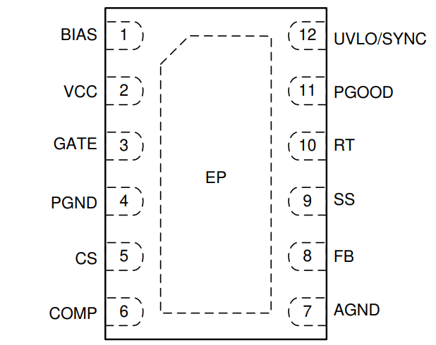
The LM5155DSSR is provided in a 12-pin WFDFN (DSS) package with an exposed pad. The table below summarizes the main functions of each pin according to the TI datasheet:
• BIAS – Supply voltage input to the internal VCC regulator. Connect a bypass capacitor from this pin to PGND.
• VCC – Output of the internal VCC regulator and supply for the MOSFET driver. Bypass to PGND with a ceramic capacitor.
• GATE – N-channel MOSFET gate-drive output. Connect directly to the external MOSFET gate through a short, low-inductance trace.
• PGND – Power ground. Return path for the switch current sense resistor and driver currents; keep the layout low-impedance and short.
• CS – Current-sense input. Connect to the positive side of the current-sense resistor through a short, low-inductance path.
• COMP – Output of the internal transconductance error amplifier. Connect the loop compensation network between this pin and PGND.
• AGND – Analog ground for control circuitry. Connect to the analog ground plane and join to PGND at a single point.
• FB – Inverting input of the error amplifier. Sense the output voltage in boost/SEPIC topologies; connect the low-side feedback return to AGND.
• SS – Soft-start timing pin. An external capacitor sets the soft-start ramp of the internal reference; connect the capacitor to AGND.
• RT – Switching-frequency setting pin. Program the operating frequency with a single resistor between RT and AGND.
• PGOOD – Power-good indicator (open-drain output). Pulls low when FB is below the regulation threshold; requires an external pull-up resistor.
• UVLO/EN/SYNC – Undervoltage lockout, enable and synchronization pin. A resistor divider from the input sets start-up/shutdown thresholds; can also accept a negative-pulse sync signal. If not used, connect to BIAS via a resistor and use an external UVLO resistor to AGND.
• EP – Exposed pad. Must be soldered to the ground copper area and connected to AGND to reduce thermal resistance and improve EMC performance.
The LM5155DSSR uses a 12-pin WFDFN exposed-pad package optimized for thermal performance and compact footprint. The exposed pad should be soldered to a ground copper area with multiple vias to internal planes to achieve low thermal resistance.
Designers should follow TI's recommended land pattern, stencil design and via arrangement from the package drawing to ensure reliable solder joints and predictable thermal behavior in volume production.
Used for 12 V/24 V boost rails, gate-driver supplies, infotainment, ADAS and body electronics modules that demand wide input range and high efficiency.
Provides robust boost/SEPIC stages in PLC I/O cards, motor-drive auxiliaries, sensors and distributed power architectures.
Generates bias rails for RF power amplifiers, optical modules and telecom line cards that require compact, reliable DC/DC conversion.
Suitable for high-density boost or flyback converters in embedded controllers, IoT gateways and battery management systems.
Engineers might also consider similar wide-VIN controllers such as:
• TI LM5156 / LM5157 family
• Analog Devices LT3757 series
• onsemi NCP3065 / NCP3066 for simpler boost stages
Texas Instruments is a leading supplier of power-management ICs with long-term product availability, extensive reference designs and strong technical support for automotive and industrial customers worldwide.
We currently provide peer-to-peer order processing. Submit an RFQ for LM5155DSSR, and our professional agent will contact you with competitive global pricing and guide you to complete the order once you accept the offer.
Our experienced QC team strictly verifies and tests LM5155DSSR. Only qualified suppliers who pass our audit can list LM5155DSSR on OEM STOCK GLOBAL LIMITED. We pay close attention to sourcing channels and product quality so you can purchase with confidence.
Pricing and inventory for LM5155DSSR fluctuate and are updated periodically (typically within 24 hours). Quotations generally remain valid for 5 days unless otherwise stated.
Wire Transfer, PayPal, Alipay, WeChat Pay, Credit Card, Western Union, MoneyGram, and Escrow are supported. Note: Some payment methods may incur a handling fee.
We support DHL, UPS, FedEx, TNT, and Registered Mail. Shipping insurance is available. After dispatch, you will receive an email with tracking information. Note: Carriers may take up to 24 hours to show tracking events. Typical transit time: 3–5 days by express; 25–60 days by registered mail.
We perform Pre-Shipment Inspection (PSI) on randomly selected units before shipping. If there is an issue with LM5155DSSR, returns/replacements are accepted when:
Steps: (1) Inform us within 90 days; (2) Obtain Return Authorization (RMA) before sending items back.
Please contact us for technical documents and support related to Texas Instruments LM5155DSSR, including pin diagrams and datasheets. Our team will respond promptly.



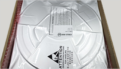
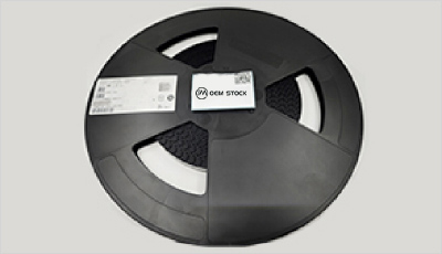
The following parts are popular search parts "LM5155DSSR" in DC DC Switching Controllers.

 Directly Purchase Of Excess Inventory
We source and manage supply to safeguard against disruption from end-of-life

 Electronic Component Consignment
We optimize supply chain operations by overseeing inventory, managing excess stock

 Electronic Component Sourcing
Global sourcing, quality assurance, and fast turnaround you can rely on.

 Electronic Component Quality Control
With rigorous process to intercept fake goods, with sincere service to deliver trust.
 Free shipping over $199
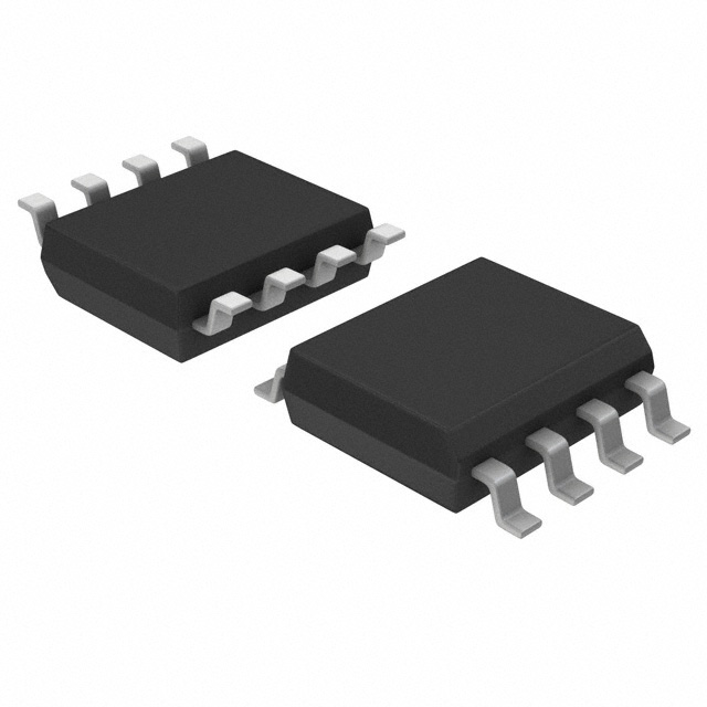
Texas Instruments
Texas Instruments
Texas Instruments
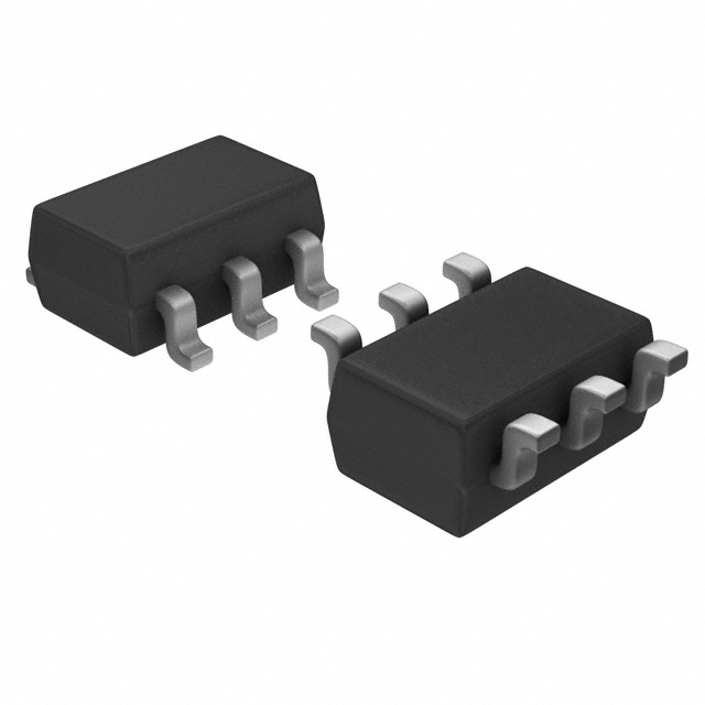
Diodes Incorporated
Texas Instruments
Texas Instruments
Microchip Technology
Texas Instruments
Texas Instruments
Texas Instruments
Texas Instruments
Texas Instruments
Microchip Technology
Texas Instruments
STMicroelectronics
Texas Instruments
 Upload