High-Speed Interfaces • Low Capacitance • IEC 61000-4-2
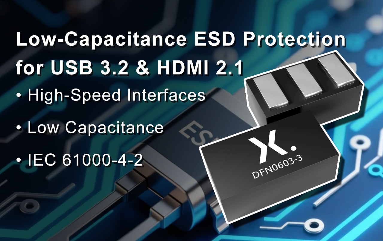
USB 3.2 and HDMI 2.1 run at multi-Gbps speeds where "strong protection" can accidentally break the link.
The goal is not only to survive ESD, but to protect signal integrity: keep eye diagrams open, maintain impedance control,
and avoid long stubs. This guide explains how engineers choose low-capacitance ESD diode arrays, how to read the key
parameters that actually matter for high-speed ports, and how to place protection so it works in the real world.
1) What threats matter on USB 3.2 / HDMI 2.1 ports?
External connectors are ESD magnets. The most common qualification reference is IEC 61000-4-2, where the discharge is
extremely fast. That speed is exactly why layout and parasitics dominate results: the discharge current finds the lowest impedance
path, and small inductances create large voltage spikes.
Field reality: Many ESD failures are not because the ESD diode is "too weak," but because the discharge current returns
through an unintended path (long ground via, thin trace, or across sensitive silicon).
2) Why low capacitance is the #1 requirement
USB 3.2 and HDMI 2.1 use high-speed differential signaling. Any protection device connected to the line adds parasitic capacitance
and introduces discontinuities. Too much capacitance can cause:
-
Eye diagram closure (reduced margin)
-
Increased insertion loss and reflection
-
Mode conversion and EMI issues
-
Intermittent link negotiation problems (hardest to debug)
Engineering principle: For high-speed ports, selecting an ESD device is primarily a signal integrity optimization problem,
while still meeting ESD robustness targets. That's why low-capacitance ESD arrays are preferred over "power TVS" parts.
3) ESD diode array types for differential pairs
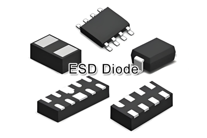
Most USB/HDMI protection uses multi-line diode arrays in compact packages. Common configurations include:
|
Array Type
|
Best for
|
Notes
|
|
Steering diode array (to VBUS/GND)
|
General high-speed signal protection
|
Requires stable rail reference; ensure rail can absorb discharge current
|
|
Rail-to-rail ESD clamp
|
Ports with defined supply rails
|
Good for low clamp, but verify rail behavior during surge
|
|
Low-cap "snapback" style ESD protection
|
Very high-speed lines needing minimal capacitance
|
Check dynamic resistance and trigger behavior; layout sensitivity is high
|
|
Dedicated differential pair protector
|
USB/HDMI optimized
|
Often specified with low insertion loss; ideal if available
|
4) Key specs engineers check (beyond "VC")
For power TVS diodes, VC and IPP are the headline specs. For high-speed ESD arrays, engineers also care about:
4.1 Capacitance (Cj) and bandwidth impact
-
Lower Cj generally improves SI, but confirm it at the relevant bias/conditions.
-
Prefer devices marketed as "low capacitance" for multi-Gbps ports.
4.2 Insertion loss / return loss (if provided)
Some vendors publish RF-style metrics. These are highly valuable because they correlate directly with compliance performance,
not just protection strength.
4.3 Dynamic resistance and clamping behavior
Fast ESD pulses can cause higher peak voltage than expected if the discharge current path is inductive or the device has high dynamic resistance.
In practice, layout + return path often dominates the peak.
4.4 Working voltage
Ensure the ESD device's working voltage fits the signal swing and common-mode range. For Type-C, pay attention to CC/SBU lines separately from SuperSpeed pairs.
Design review tip: If you can only validate two parameters: verify Cj (low) and verify placement for short stubs + strong ground.
5) Placement rules that decide pass/fail
ESD is a current event. The ESD diode only works if the discharge current is routed into it quickly and returned to ground with minimal inductance.
Use these rules:
-
Place ESD array right at the connector pins (often within a few mm).
-
Minimize stub length between the diff pair and the ESD pad (avoid long "T" branches).
-
Use multiple ground vias at the ESD device (stitch into a solid plane).
-
Keep the return path short and wide; avoid thin traces for ESD return.
-
Route differential pairs with consistent impedance; avoid sharp corners and layer swaps near the ESD part.
Experience-based note: It's common to see a "good" ESD device behave poorly simply because there is a long via-to-plane distance.
Adding vias and shortening the return path often improves robustness more than changing part numbers.
6) Typical port protection topologies
6.1 USB 3.2 (Type-C) practical topology
-
Low-cap ESD arrays on SuperSpeed differential pairs near the connector
-
Separate ESD protection for CC and SBU pins (different voltage behavior)
-
VBUS protection handled by a power TVS near the power entry path, not on the high-speed pairs
6.2 HDMI 2.1 topology
-
Low-cap ESD arrays for TMDS/FRL lines close to connector
-
Solid shield/chassis grounding strategy at connector shell
-
If using common-mode chokes, place them according to SI goals and ensure the ESD device still sees the discharge first
Layered protection concept: Use power TVS where energy is high (VBUS, rails), and low-cap ESD arrays where speed is high (data pairs).
7) Common mistakes (and how to avoid them)
-
Mistake: Using a high-power TVS diode on USB/HDMI data lines.
Fix: Use low-capacitance ESD arrays; check insertion loss if available.
-
Mistake: ESD device placed far from connector "for routing convenience."
Fix: Place ESD device at connector, then route inward. Prioritize protection topology.
-
Mistake: Only one ground via or thin ground trace at ESD device.
Fix: Use multiple stitching vias and wide copper to the ground plane.
-
Mistake: Long stubs and poor differential symmetry at the ESD tap point.
Fix: Keep stubs short and symmetrical; maintain controlled impedance.
-
Mistake: Ignoring connector shell / chassis strategy.
Fix: Define a clear return path for ESD at the mechanical boundary.
8) FAQ
Q: Do low-cap ESD diodes provide "enough" protection?
A: For IEC 61000-4-2 style ESD, yes-when placed correctly with a strong return path. Layout and grounding often determine the real peak voltage.
Q: Should I protect both lines of a differential pair?
A: Yes. Use a device intended for differential pairs or matched channels to minimize imbalance and mode conversion.
Q: What if my design still fails ESD after adding an ESD array?
A: Check the return path first: ground vias, plane continuity, stub length, and connector shell strategy. Those fixes often outperform part swaps.
 Upload