1) Why LM3489 works well for efficient buck designs
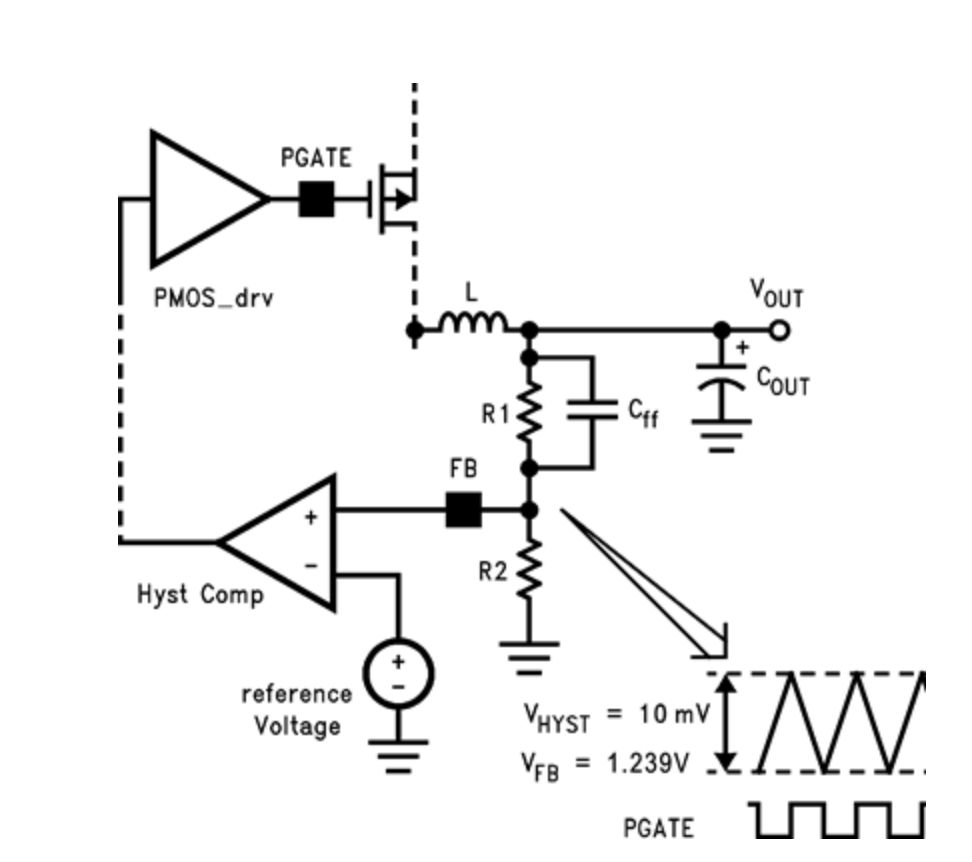
High efficiency in a buck converter usually comes down to three buckets: conduction losses (RDS(on), DCR, diode Vf), switching losses (gate charge, rise/fall times, ringing),
and layout/EMI cleanliness (hot-loop inductance, switch-node noise coupling).
-
PFET high-side approach can simplify the power stage (no high-side bootstrap driver) and supports
near-dropout operation when VIN approaches VOUT (useful for battery rails).
-
Hysteretic control can respond quickly to load transients and avoids the "compensation design" workload.
The tradeoff is that switching frequency is not fixed-it varies with ripple thresholds and your L/C choices.
-
Cycle-by-cycle current limiting is typically implemented by sensing PFET RDS(on) (or a sense resistor if you
need better accuracy).
Practical note: hysteretic converters can be extremely robust, but only if the power stage and PCB layout are treated as
part of the control system. "Good layout" is not optional.
2) Define requirements (the part most designs skip)
Before selecting any component, write the operating envelope. You'll avoid re-spins if you define these up front:
-
VIN range: minimum / nominal / maximum (include surges if your system sees spikes).
-
VOUT target: regulation tolerance and ripple limit.
-
IOUT profile: continuous load, peak load, transient step size and edge rate.
-
Efficiency targets: at which points (10%, 50%, 100% load) and at which VIN values.
-
Thermals: ambient range, airflow, copper area available under PFET/diode, enclosure constraints.
-
EMI constraints: if you have compliance targets, plan layout and filtering early.
3) Set the output voltage (FB/ADJ divider)
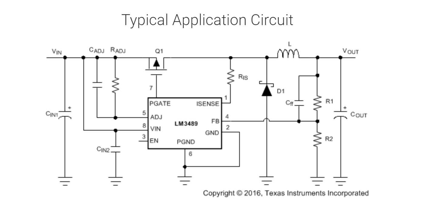
LM3489 regulates its feedback node to an internal reference. You set VOUT using a resistor divider:
VOUT = VREF * (1 + Rtop / Rbottom)
Divider current matters. If resistors are too large, the FB node becomes noise-sensitive. If too small, you waste power.
A common starting point is Rbottom in the tens of kΩ, then compute Rtop. Final values should be validated on hardware.
4) Select the PFET (biggest efficiency lever)
For high efficiency, PFET choice is usually the biggest lever because it impacts both conduction and switching loss.
Here's how to choose it like a power designer:
-
RDS(on) at temperature: check the curve, not just the 25°C headline number. High-load efficiency is often dominated here.
-
Gate charge (Qg): lower Qg improves switching loss and light-load efficiency, but may increase RDS(on). You want the best overall trade.
-
VDS rating: include real margin. Switch-node ringing and cable inductance can create spikes above VIN.
-
Low-VIN behavior: ensure the PFET is fully enhanced at your minimum VIN and gate drive headroom.
Engineering workflow tip: When you move from schematic to BOM, validate decisions against a real controller SKU and package constraints.
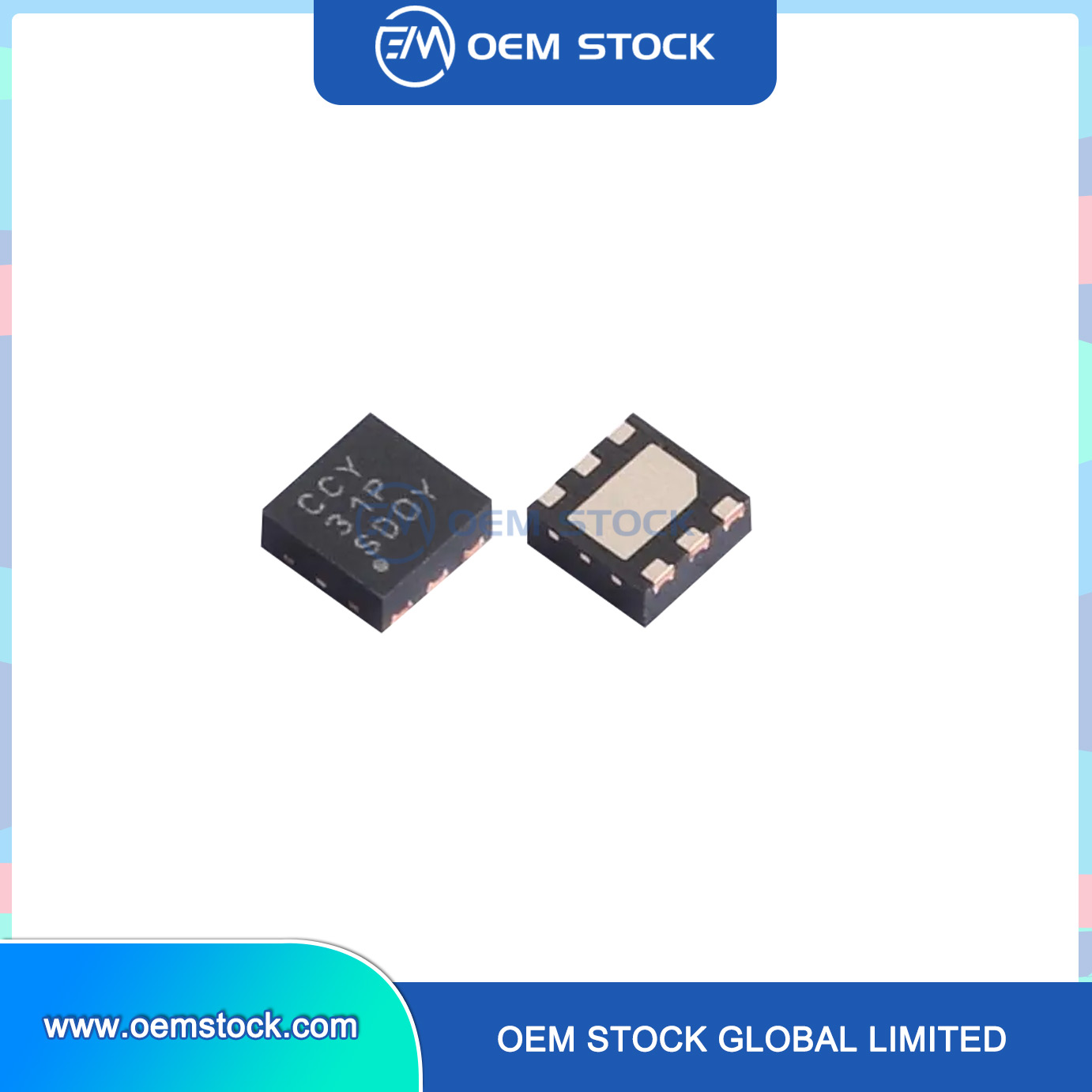
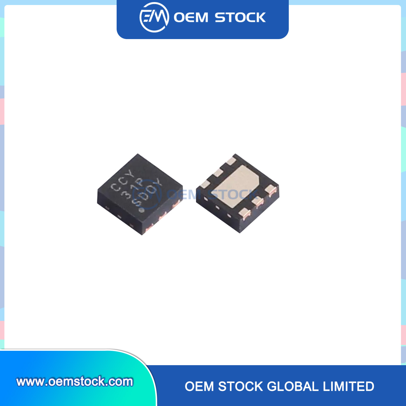
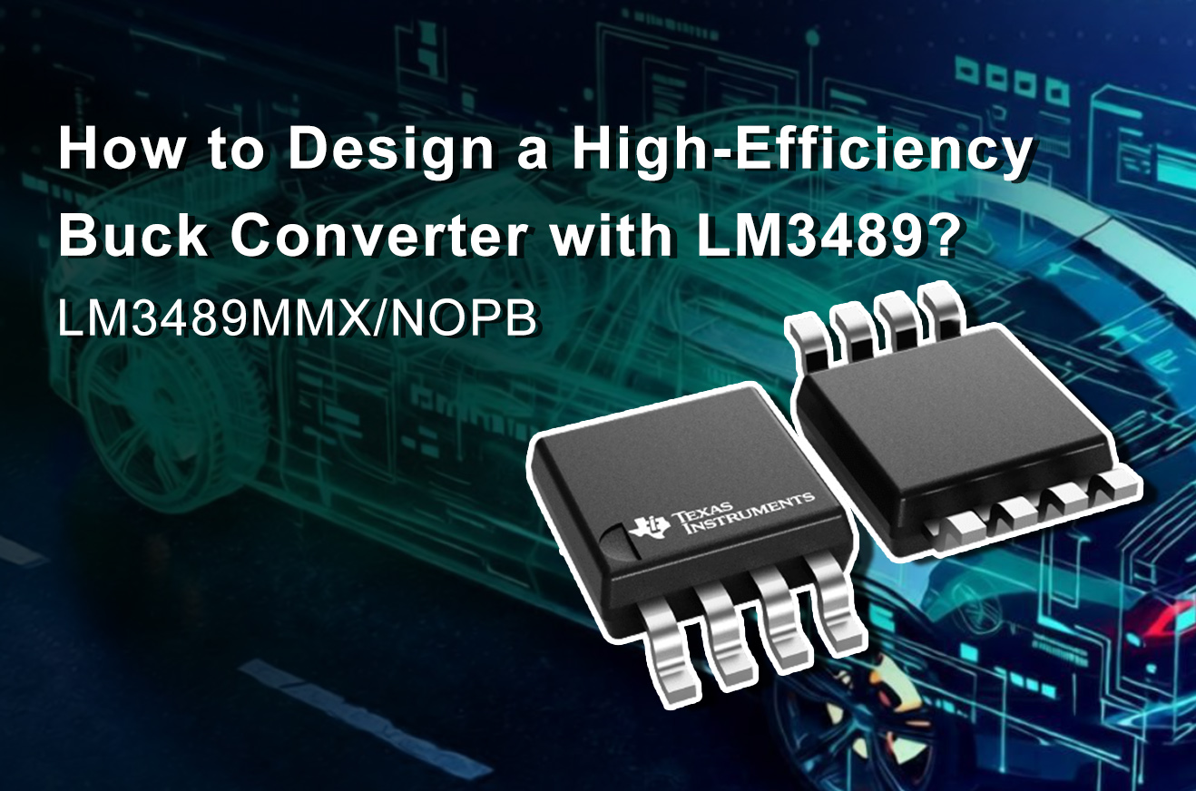
If your design will be built around LM3489MMX/NOPB,
confirm the footprint, thermal copper strategy, and proximity of CIN/COUT to match the switching current loops.
5) Inductor selection (ripple, saturation, DCR)
Inductor selection is a balance: ripple current, transient response, size, and losses.
A practical target for ripple current is often 20%–40% of IOUT(max).
Estimate inductor ripple current
ΔIL ≈ (VOUT / L) * (1 - VOUT/VIN) * (1/fsw)
With hysteretic controllers, the effective switching frequency (fsw) is not fixed.
Use this equation for sizing, then measure the real ripple and frequency on hardware.
Inductor checklist
-
Saturation current: must exceed peak inductor current (IOUT(peak) + ΔIL/2) with margin.
-
DCR: lower DCR improves high-load efficiency but may increase size/cost.
-
Core losses & audible noise: watch for whine at light load or under certain operating points.
6) Catch diode selection (Schottky)
You still need a catch diode to provide the freewheel path when the PFET is off.
For efficiency and switching cleanliness, a Schottky diode is usually the default choice.
-
Low forward voltage (Vf) improves efficiency, especially at higher currents.
-
Current rating should cover load and transient conditions with thermal margin.
-
Reverse voltage rating should exceed VIN with margin.
High VIN designs are more sensitive to switch-node undershoot and ringing; diode selection and layout become even more critical.
7) Input/output capacitors (ripple + transient performance)
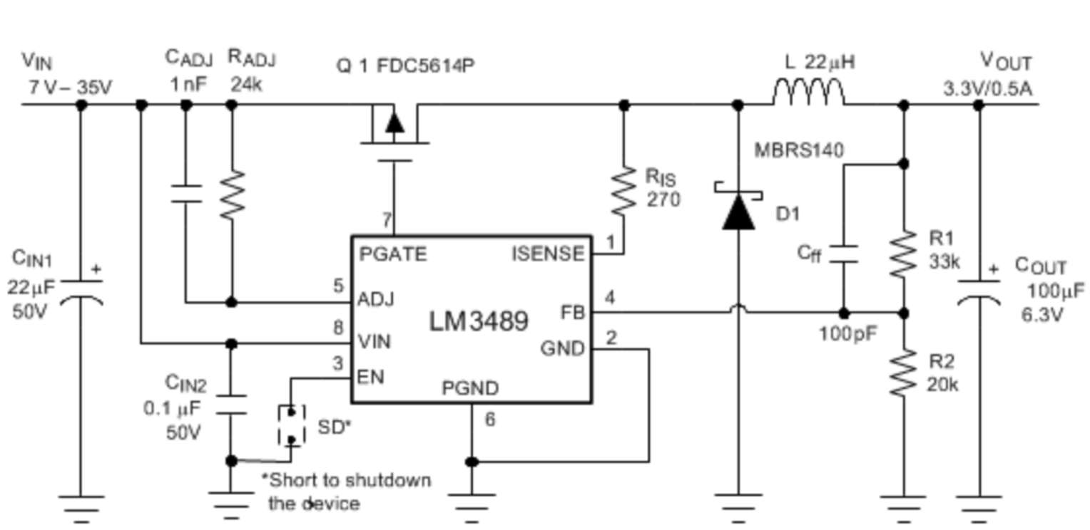
Capacitors do more than "reduce ripple." They define current loops, influence switching stress, and shape transient performance.
A reliable approach is to use:
-
CIN: a tight ceramic close to the PFET + controller, plus bulk if the source impedance is high (long cable, connector, upstream rail).
-
COUT: a bulk capacitor for load-step energy, plus ceramics near the load for high-frequency ripple control.
What to watch for
-
Ceramic DC-bias derating: your "10 µF" might be far less at operating voltage.
-
ESR/ESL: affects ripple and ringing; placement matters as much as value.
-
Thermal aging: polymer electrolytics and ceramics behave differently over time and temperature.
Practical disclaimer: all capacitor values are starting points. Final selection should be validated on real hardware across
temperature, load, and input voltage extremes.
8) Current limit setup (ISENSE/ADJ)
Current limiting is typically implemented by sensing the PFET's RDS(on) (which can remove the need for a sense resistor),
but a sense resistor can be used if you need higher accuracy. Treat current limit as a safety function and verify it across
temperature and tolerance.
-
Validate current limit at VIN(min), VIN(nom), VIN(max).
-
Check the short-circuit response and whether your input rail sags or oscillates under fault.
-
Observe the switch node with correct probing technique (short ground spring) to avoid "measurement ghosts."
9) PCB layout rules that matter
Layout will make or break your efficiency and stability. The key is to minimize loop inductance in the switching paths and
keep sensitive nodes away from the noisy switch node.
Critical layout checklist
-
Minimize the hot loop: CIN → PFET → SW node → diode → GND → back to CIN.
-
Place CIN close: the ceramic input capacitor must be physically close to the PFET/controller power pins.
-
Keep SW copper small: reduce EMI, ringing, and noise coupling into feedback traces.
-
Separate power and signal ground: join at a quiet point near the controller ground reference.
-
Route FB/ADJ cleanly: keep away from SW; avoid running underneath the switch node plane.
-
Thermal copper: give PFET and diode enough copper area; confirm temperature rise in worst-case ambient.
10) Worked example flow (12 V → 5 V / 2 A)
Below is a production-friendly design workflow. The goal is not to guess perfect values on paper, but to converge quickly with
a controlled set of measurements.
|
Step
|
Decision
|
Bench verification
|
|
1
|
Set envelope: VIN 9–16 V, VOUT 5.0 V, IOUT 2 A, ripple target
|
Start-up, line regulation across VIN range
|
|
2
|
Lock controller SKU & footprint (e.g., LM3489MMX/NOPB)
|
Pinout/footprint check, thermal copper strategy, placement constraints
|
|
3
|
Select PFET: low RDS(on) at temperature + reasonable Qg, VDS margin
|
PFET temp at full load, efficiency sweep at light/medium/full load
|
|
4
|
Pick inductor: target 20–40% ripple; ensure saturation margin and DCR trade
|
Measure ripple current and effective switching frequency
|
|
5
|
Choose Schottky diode: low Vf + thermal headroom
|
Diode temperature rise and switch-node ringing behavior
|
|
6
|
Set COUT/CIN: bulk + ceramics; keep CIN close to hot loop
|
Load-step droop/overshoot, ripple under typical load
|
|
7
|
Configure current limit (ISENSE/ADJ) and validate fault response
|
Short-circuit tests, current limit threshold across VIN & temperature
|
11) Troubleshooting guide
Symptom A: Output ripple is higher than expected
-
Add ceramic capacitance close to the load (short traces).
-
Increase inductance slightly (tradeoff: transient response and size).
-
Confirm FB/ADJ routing is not coupling to the SW node.
Symptom B: Audible noise / "wandering" frequency
-
Check inductor saturation and core material selection.
-
Verify ceramic DC-bias derating-effective capacitance may be lower than expected.
-
Reduce hot-loop area and shrink the SW copper region.
Symptom C: Unexpected heating at full load
-
PFET: RDS(on) at temperature may be higher than assumed-recalculate conduction loss and verify copper area.
-
Inductor: DCR loss may be dominating-consider a lower-DCR inductor if size allows.
-
Diode: Vf and thermal impedance may be limiting-upgrade diode or improve copper heat spreading.
12) Final validation checklist
-
Efficiency sweep at 10%, 50%, 100% load across VIN(min/nom/max).
-
Thermal test in worst-case ambient: PFET, diode, inductor, controller area.
-
Load transients: step up/down; record overshoot/undershoot and recovery time.
-
Switch-node ringing: confirm probe technique; reduce ringing via layout and component placement first.
-
Fault behavior: current limit, short-circuit response, restart behavior (system-dependent).
From design to production
Once your schematic values look reasonable, the fastest path to a production-ready converter is:
build a first PCB with conservative placement, measure efficiency/thermals/ripple, then iterate only the parts that move the needle
(usually PFET selection, inductor DCR vs size, and capacitor placement).
After bench validation and thermal testing, lock the controller part number used in production.
Choosing a widely available, production-grade device such as LM3489MMX/NOPB helps reduce sourcing risk and keeps future maintenance straightforward.
FAQ
Is LM3489 a fixed-frequency controller?
No. LM3489 uses hysteretic control, so the effective switching frequency varies with ripple thresholds and your L/C network.
That's why you size components with estimates and then verify ripple and frequency on hardware.
Can I implement current limit without a sense resistor?
In many designs, yes-current limit can be implemented by sensing the PFET's RDS(on). If your application requires tighter accuracy,
a sense resistor approach may be more predictable across tolerance and temperature.
What's the biggest mistake that reduces efficiency?
Two common efficiency killers are: (1) choosing a PFET that looks good at 25°C but runs hot at load, and (2) poor layout that creates
ringing and extra switching loss. Start with the PFET + layout fundamentals, then refine the passives based on measurements.
Should I link the guide to a specific part number?
Yes-if done naturally. Linking to the exact SKU (for example LM3489MMX/NOPB)
helps readers verify packaging, availability, and BOM alignment without turning the article into an advertisement.
About the Author
This article is written from a practical power-design perspective, focusing on DC-DC converter selection,
PCB layout optimization, and verification steps (efficiency, ripple, thermals, and fault behavior) that matter in production.
References (recommended)
-
Texas Instruments LM3489 datasheet
-
LM3489 evaluation / demonstration board documentation
-
General DC-DC layout and measurement best practices (probe technique, hot-loop minimization)
Tip: If you publish this on OEMSTOCK, also add an internal link on the product page pointing back to this guide.
That "two-way link" improves discoverability for both information-intent and purchase-intent visitors.
 Upload